
4.1 KiB
Maze Solver Chip Design Report
An explanation of the design of our 16x16 expandable maze solver chip, including a detailed dive into the SystemVerilog.
1. High-Level Chip Purpose and Design
The chip is able to solve a maze by requesting cell locations from off-chip memory and intaking their wall configurations as a 4-bit input.
- As the chip moves around the maze, it requests new memory locations until it reaches the end of the maze.
- The chip may take dead-end paths, but its solution does not include any dead ends due to the implementation of a hardware stack.
- Once it eaches the end, the chip outputs the solution as a series of 2-bit numbers corresponding to the series of moves (up, right, down, left) needed to successfully traverse the maze.
2. FSM and General Flow
FSM Implementation
The chip's controller is a 14-state FSM. The FSM state diagram is shown below.
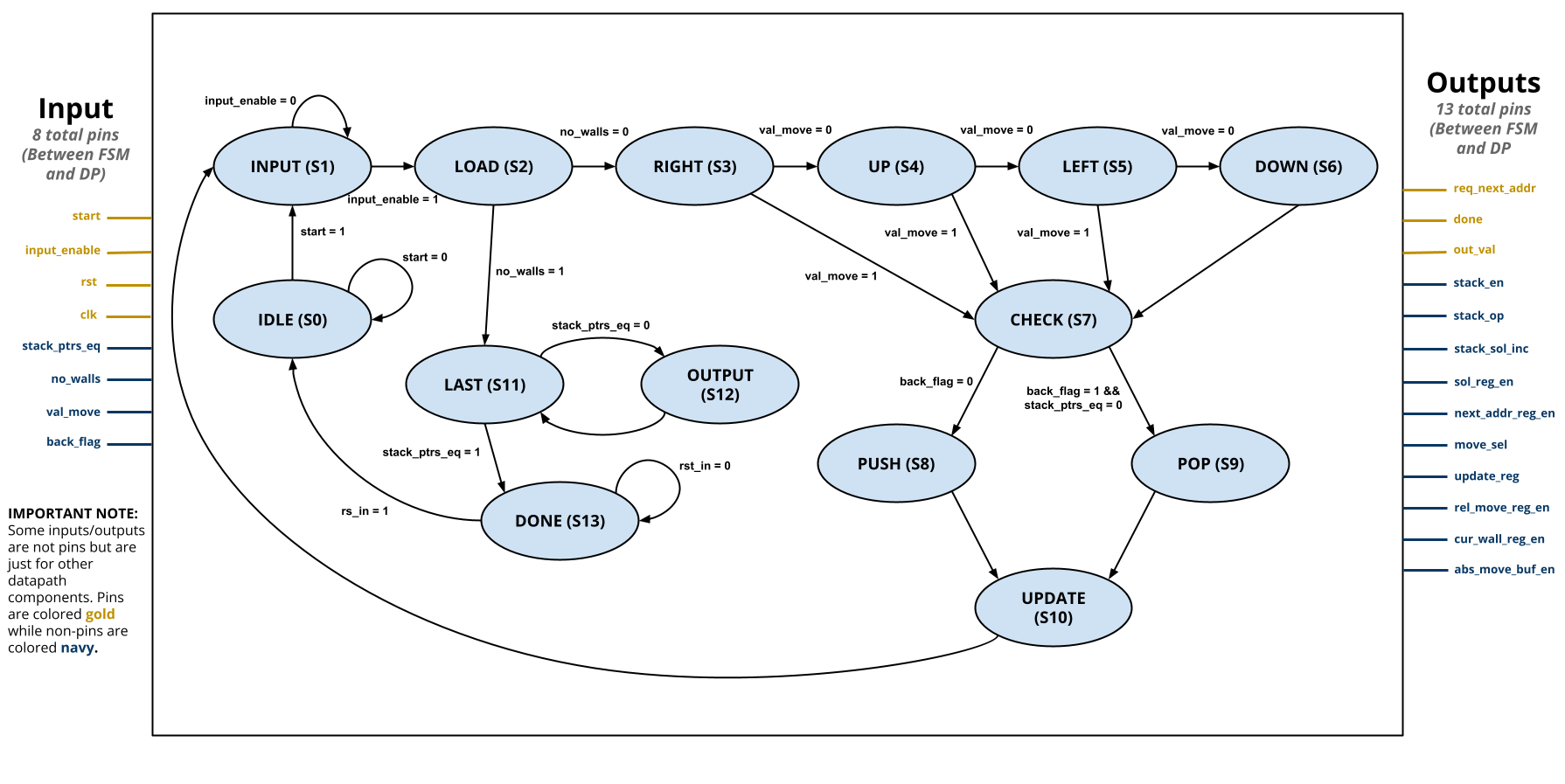 Note: only inputs and outputs to the FSM are shown, not the datapath.
General Flow
This is the general flow of the chip:
Setup
- IDLE (S0): Wait for the external start input pin to go high before proceeding. Then go to INPUT (S1).
Intake Walls
- INPUT (S1): Wait for the external input_enable input pin to go high, indicating that input cur_wall [3:0] is valid for the requested address req_addr [7:0] output. Then go to LOAD (S2).
- LOAD (S2): Save cur_wall [3:0] input at the start of the datapath. If the input is 0000, we've reached the end so jump to LAST (S11); otherwise, continue to RIGHT (S3).
Move Decision
- RIGHT (S3): Check to see if a right turn is possible. If so, go to CHECK (S7); otherwise, continue to UP (S4).
- UP (S4): Check to see if going straight is possible. If so, go to CHECK (S7); otherwise, continue to LEFT (S5).
- LEFT (S5): Check to see if a left turn is possible. If so, go to CHECK (S7); otherwise, continue to DOWN (S6).
- DOWN (S6): This move will always be possible (for details, see datapath section). Go to CHECK (S7).
Backtrack Detection
- CHECK (S7): Check to see if current move is is backtracking on a previous move. If so, go to POP (S9); otherwise, go to PUSH (S8).
- PUSH (S8): Push the current move to the stack. Go to UPDATE (S10).
- POP (S9): Pop from the stack. Go to UPDATE (S10).
- UPDATE (S10): Update internal registers in preparation for next cycle. Go to INPUT (S2).
Output Solution
- LAST (S11): Check to see if the last move has been read. If so, go to DONE (S13); otherwise, go to OUTPUT (S12).
- OUTPUT (S12): Read value from stack, starting from the bottom, to the solution [1:0] output. Go to LAST (S11).
- DONE (S13): Wait for external rst signal to go back to IDLE (S0).
3. Code Organization
Our maze solver code is organized hierarchically as follows:
    // FSM declaration
    module fsm_design;

    // Datapath component declarations
    module reg_nbit;
    module add_sub_wrap_nbit;
    module not_left_nbit;
    module bit_sel_4bit;
    module not_4bit;
    module nor_4bit;
    module move_conv_logic;
    module back_test_logic;
    module split_1_to_2_nbit;
    module stack_ncell;

    // Datapath declaration
    module datapath_design (
       	reg_nbit cur_wall_reg,
       	rot_left_4bit rotate_wall,
       	reg_nbit abs_dir_reg,
       	not_4bit wall_invert,
       	bit_sel_4bit test_move,
       	nor_4bit wall_check,
        reg_nbit rel_move_reg,
        reg_nbit abs_move_buf,
        reg_nbit rel_to_abs_alu,
        move_conv_logic move_conv,
        add_sub_wrap_nbit cur_to_next_alu,
        reg_nbit cur_addr_reg,
        reg_nbit next_addr_reg,
        split_1_to_2_nbit addr_split,
        back_test_logic back_test,
        stack_ncell stack,
        reg_nbit sol_reg
    );

    module chip_design (
        fsm_design controller,
        datapath_design datapath
    );
Our highest-level module, chip_design, is at the bottom of the .sv file to preserve Verilog hierarchical organization rules, where the components of a module are declared above the module.
4. Datapath
This is our circuit diagram:
